
Reading time: 3 minutes
Text: James Woodcock
Semiconductor production runs on laser optics, inspection systems and measurement equipment held to very tight tolerances. Microscopic particle deposits can be enough to degrade accuracy and push up maintenance requirements. The usual defenses are air purging, extraction or vacuum assistance, each adding kit and complexity to a system already short of space.
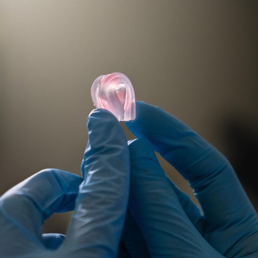
Sinto Advanced Ceramics Europe has taken a different route with an optical protection cap carrying three functions in one additively manufactured body. Alongside the physical shield, internal channels generate a targeted vacuum that draws particles and process residues away from the optical path. Mounting and fastening features sit in the same geometry.
The component measures 20 by 20 millimeters with a height of 6.5 to 12 millimeters, produced in yttrium-stabilized zirconia by ceramic stereolithography. Equipment inside a chip fab can become a contamination source as it wears, so alongside strength and fracture toughness the wear resistance of technical ceramics keeps particle generation low.
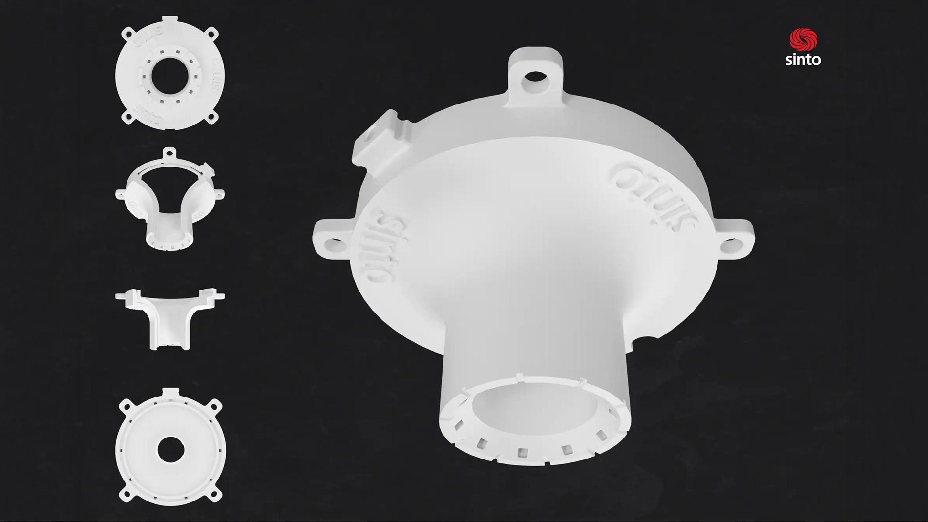
The company puts its design principle plainly: geometry follows performance requirements rather than tooling constraints or machining directions. Channel layouts can be revised in CAD for different optical systems without new tooling.
The Immenstadt firm, formerly Bosch Advanced Ceramics, joined the Sintokogio Group in January and shows the cap at Semicon Europa in Munich in November.
Further information