

6 March 2023, by Thomas Masuch
Whether it was in smart tools or a full-on revolution in circuit boards, the amount of promise ascribed to the 3D Printing of electronics was almost fanciful just a few years ago. After all, this still-nascent field does present tremendous potential in various areas of application – think of the automotive, microchip, aerospace, or tool-building industries, for instance. While the initial hype has certainly cooled, such methods of AM are now making gradual progress toward industrial use.
The way the 3D printing of electronics has evolved has parallels with the early days of additive manufacturing itself. On the one hand, there are promising ideas, ambitious visions, and some actual completed components; on the other, plenty of challenges still need to be overcome. Meanwhile, more and more people and companies are exploring the subject, both as users and providers of technology.
The increased importance of 3D-printed electronics was perhaps nowhere more apparent than at Formnext 2022, where various exhibitors – including Nano Dimension, Optomec, J.A.M.E.S, and a number of Fraunhofer institutes – demonstrated printers and forward-thinking applications in the field. “In terms of perception, the momentum has really been building over the past six to 12 months,” affirms Alexandre Schäfer, business development manager at J.A.M.E.S, a young platform that operates in additively manufactured electronics (AME). “Every single person who joins our online community is priceless when it comes to getting new ideas off the ground.”
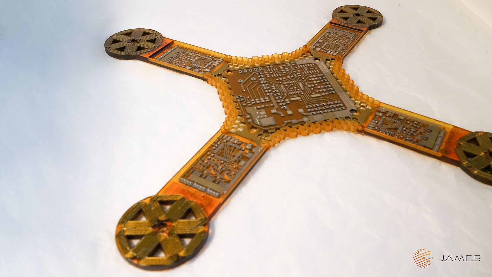
The examples of ways in which 3D-printed electronics can be used are already getting hard to count, ranging from more efficient electric motors (for which the company Additive Drives prints three-dimensional coil forms) to 3D-printed antennas that see use in spaceflight (an amplifier module has already been in orbit on the ISS). Just one of the paths the evolution of AME could take has been charted by J.A.M.E.S, whose innovations include a 3D-printed drone assembly platform that supports circuit paths, motor coils, and other electronic components. These are printed on a DragonFly IV from Nano Dimension using silver nanoparticle ink, while the platform itself is manufactured from a photopolymer.
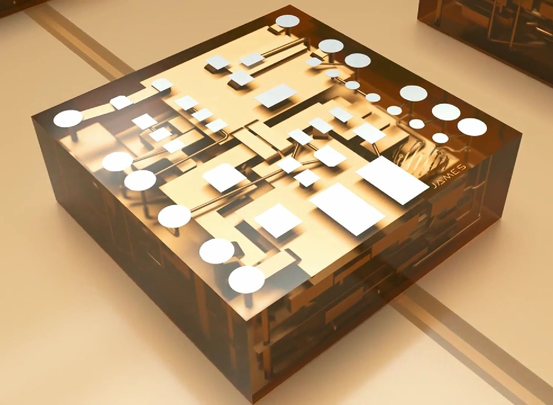
With this PLL cube, J.A.M.E.S has shown one path future AME applications might follow: At higher levels of stability, any available space can be filled with electronics or dielectric materials. Image: J.A.M.E.S
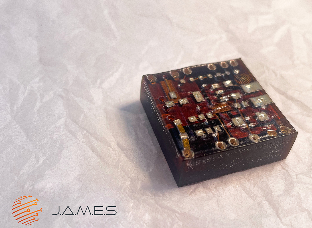
With this PLL cube, J.A.M.E.S has shown one path future AME applications might follow: At higher levels of stability, any available space can be filled with electronics or dielectric materials. Image: J.A.M.E.S
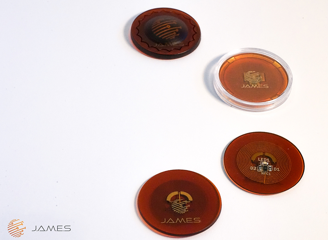
The J.A.M.E.S Coin is a near-field communication tag that demonstrates a way to print antenna coils and free-formed plate capacitors under the strictest space limitations. Image: J.A.M.E.S
“Showing what’s possible“
Acknowledging that it still takes quite a while to print a drone at the moment, Schäfer points out that the team at J.A.M.E.S mainly wants to show what’s possible. “We had lots of people visiting our Formnext booth who didn’t realize this could be done and were pretty excited to see it,” he says. Some of these new converts were from the mechanical engineering sector, where manufacturers of CNC machines in particular are having to integrate more and more electronics into their products. For design reasons, the amount of space available inside such machines is limited, which sometimes makes it impossible to squeeze in more circuit boards. “With 3D printing, you can combine the components of all your circuit boards in a 3D-printed part that also has ventilation built in, for example, which solves the issue of heat dissipation at the same time,” Schäfer explains.
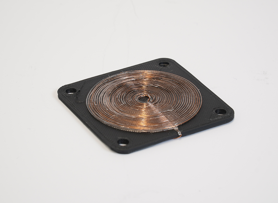
J.A.M.E.S, a network founded by Hensoldt and the aforementioned Nano Dimension, already has in-house expertise in applications like these. At Formnext, it demonstrated another method of printing electronics onto a component in very tight spaces with the J.A.M.E.S. Coin – a near-field communication tag that incorporates an antenna coil and free-formed plate capacitors into a tiny disc.
The applications J.A.M.E.S is currently overseeing are based mainly in the areas of research, aerospace, and defense, which can be attributed to Hensoldt’s involvement. The Bavarian company specializes in radar, optronics, and avionics and has been working on 3D-printing electronic components since 2016.
Patience and perseverance
Although AME is still in its early stages, this area of additive manufacturing has already passed through its initial hype phase. Much of its development is reflected in that of Nano Dimension, a leading manufacturer of 3D printers for electronics. Following its foundation in 2012, the Israeli firm went public on the NASDAQ to much fanfare in 2016 and achieved a market cap of well over U.S.$20 billion. In the meantime, however, its share price has plummeted from over U.S.$90 to around U.S.$2.50.[1] Nano Dimension has nonetheless stayed the course and continued to develop its technology, which has resulted in constant growth in machine sales of late.
[1] as of 10 February 2023
As was the case in the early days of “traditional” additive manufacturing, it appears that a good bit of patience and perseverance will be required before AME fulfills the lofty expectations that have been placed on it. “In terms of our technical readiness level, we’re between four and six, meaning just after the prototyping phase,” Schäfer reports. “Unfortunately, we’re still a long way from serial production.”
It’s no wonder the AME market is still rather modest in size. According to Schäfer, many potential users are shying away from buying their own printers due to the unpolished state of the current technology and opting to work with research partners instead. “We expect that to change as the technology gets more and more mature,” he says. One of the reasons why progress isn’t being made more quickly has to do with the complex manufacturing technology involved, as Schäfer’s colleague, J.A.M.E.S CTO Andreas Salomon, explains. “In AME, we’re taking 3D printing to the next level, which is the electrification of volumes,” Salomon says. “We’re dealing with the printing of not only multiple materials, but conductive and non-conductive structures, as well. That makes it more complex on the whole than conventional additive manufacturing.”
Printed electronics, or built-in?
“Our goal is to manufacture electronic components that are entirely 3D-printed, all the way down to the circuit paths,” Schäfer declares. This involves the use of silver and copper paste, conductive functional fluid, and special synthetics, or even ceramic. Meanwhile, other companies and research institutes are taking a somewhat more technologically feasible route. Instead of 3D-printing electronics, they incorporate such components into the 3D printing process. Such parts are inserted into semi-finished components (“pick-and-place”), typically in a manual fashion.
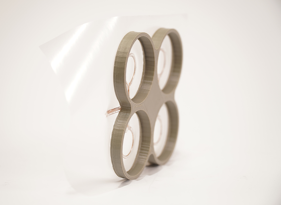
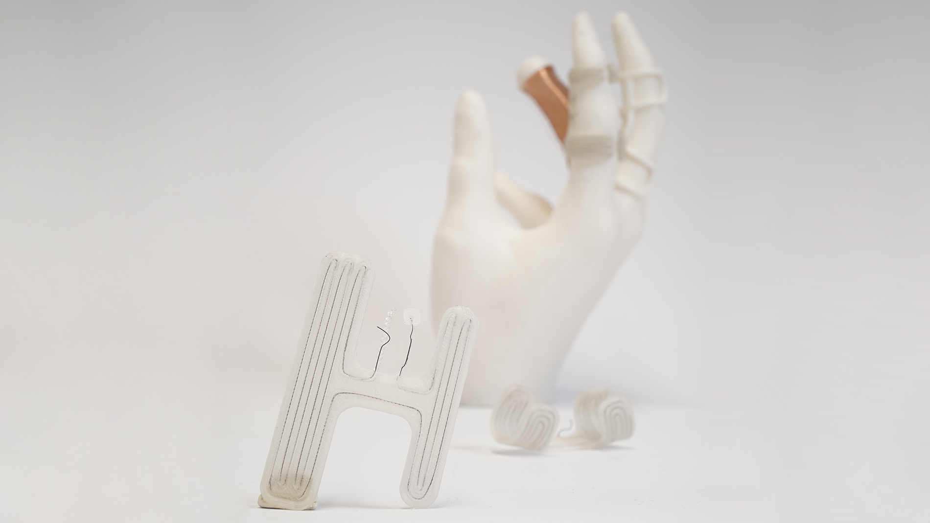
Various electronic applications from Fraunhofer IWU: 200-μm copper wire on 100-μm film with printed on structural components….
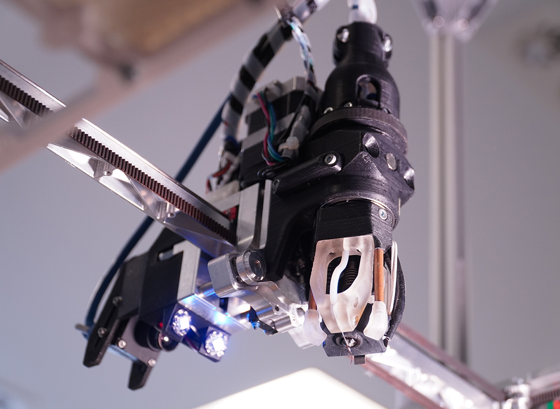
a WEAM printer head with integrated process monitoring, and….
an induction coil on ABS. Images: Fraunhofer IWU
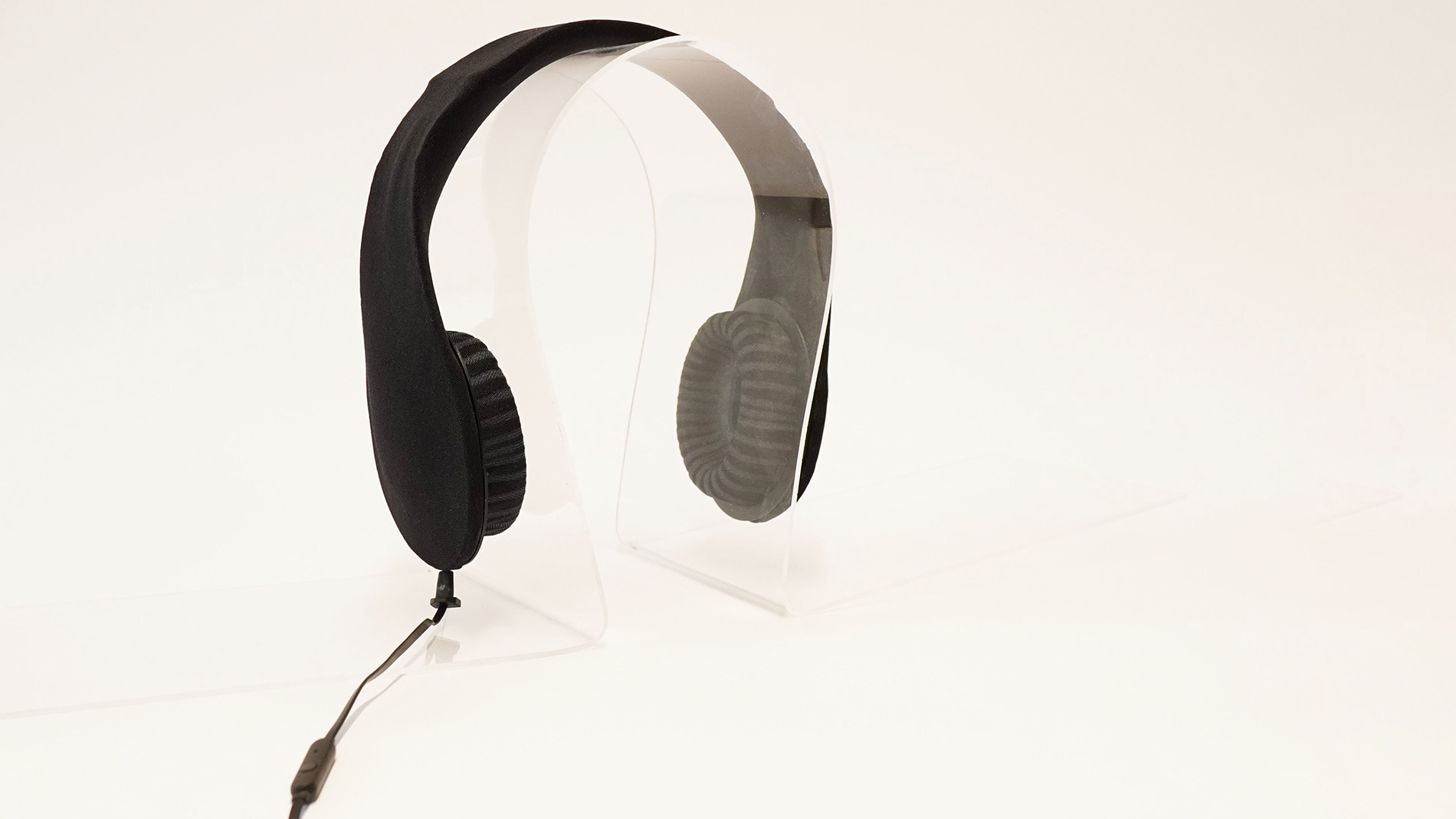
For proof that this could also open the door to new areas of application, look no further than the Fraunhofer Institute for Machine Tools and Forming Technology (IWU) in Dresden, Germany. Here, the insertion and mounting of circuit boards, wires, and magnets is combined with multi-material printing and fully automated in a corresponding production system. This presents a broad range of research applications, including in connection with individual cable wiring harnesses, electric drive systems, or speakers that are completely 3D-printed. The IWU showcased the latter at Formnext 2022 in Frankfurt am Main, and the subject resonated with a great many attendees. “People were already asking how they could get one of these systems,” reveals Lukas Boxberger, head of the biomechatronics division at the IWU.
“The wire encapsulation additive manufacturing (WEAM) technology we’ve developed and the integration of electronic components represent a huge expansion of the range of possible AM applications. Ultimately, they make it possible to manufacture not only structural parts, but entire products like battery-powered screwdrivers or other handheld devices.”
Boxberger also believes that the ability to integrate wiring into plastic components will open up even more areas of use. Doing so makes it possible to heat parts like these from the inside and make them malleable, which would take much of the effort out of customizing things like orthotic leg braces. Better yet, the process could be repeated again and again to make geometric adjustments, such as when a wearer’s muscles increase or decrease in size as part of the healing process or a limb absorbs water throughout the day. “That’s a significant improvement on the current state of the art,” Boxberger points out. He adds that the automotive industry would be another space in which it would be possible to modify prototypes in just a few steps or integrate functions related to sensors, data, power routing, or heating directly into components. “Overall, this technology makes it much easier to develop complex products.”
Scientific foundation now in place
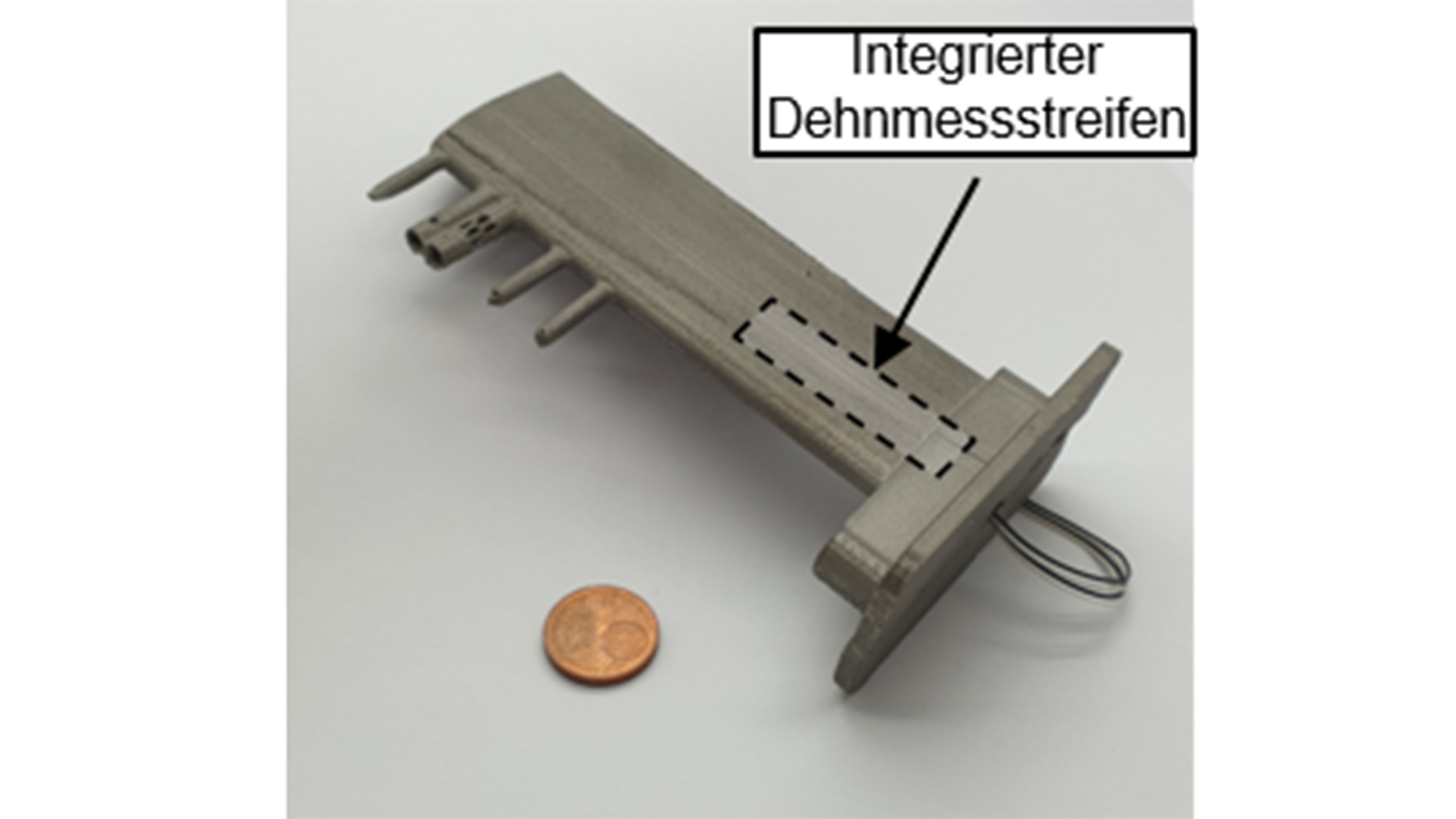
Electronics can also be incorporated into 3D-printed metal parts, as the Fraunhofer Institute for Casting, Composite, and Processing Technology (IGCV) showed in a recent study. In it, Fraunhofer integrated a sensor into 3D-printed steel gearwheels. “Usually, the printing process has to be interrupted to insert sensors like these,” explains Prof. Christian Seidel, head of additive manufacturing at the IGCV, which took another step toward industrialization in the project. “We showed that it can also be done automatically using a PBF machine and without disrupting the inert atmosphere, which normally results in lower-quality components.” According to Seidel, printing electronics into metal parts is more challenging, but it offers the advantage of being able to place sensors right where you want them.
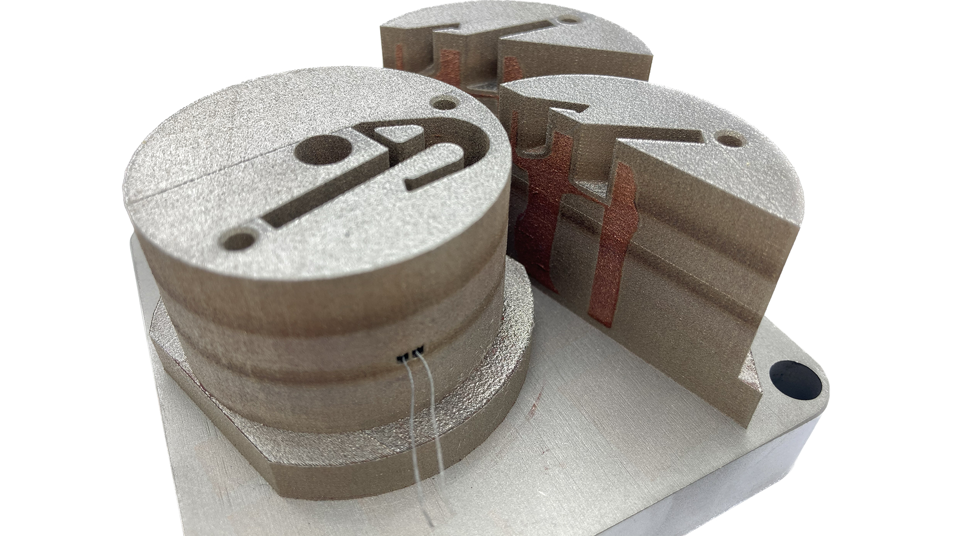
A machine can also be automated in this way on a relatively low budget, Seidel says. “In practically the same amount of production time, you can make a smart component.” The other applications the AM chief has researched at Fraunhofer IGCV include integrating an additional vibration sensor into a 3D-printed measurement device and 3D-printing a multi-material injection mold in which some sections were made of copper to optimize the mold’s heat transferring properties. A sensor was also incorporated into the mold to monitor its temperature during the process and fine-tune the production speed.
Although there aren’t many applications being used in industrial settings at the moment, Seidel sees a great deal of potential in additively manufactured electronics. “We’ve laid the scientific foundation and published our work,” he says. “The more word gets around about this subject, the more innovations will follow.” As for the level of interest in this type of integration in the wider world of AM, Seidel points to his experience at Formnext 2022: “Our booth had a huge influx of people wanting to find out more.”
That said, the professor stresses that assembling a corresponding production setup is hardly trivial. Machine upgrades, choosing the right sensors, the printing process itself, and much more require a high degree of expertise. “As of now, there’s also no plug-and-play solution on the market,” Seidel adds. “For that to change, manufacturers have to be willing to take on projects with industrial partners in order to show the market potential of this technology.”
Big business beckons in circuit boards and chips
To continue driving these innovations, Andreas Salomon from J.A.M.E.S believes the networking approach is the right way forward. “The technology is so complex and requires so much development effort that it’s not really manageable for a single company,” he explains.
The practically endless scope of possible applications – and the sheer size of the potential market –indicate that that effort will be worth it, however. Right now, developments are under way in fields like medical technology, and in defense under the theme of “the soldier system” (which involves things like wearables and telemetry sensors that monitor performance data during missions). According to Salomon, though, the potential market in circuit boards and chips is the largest by far. He points out that since establishing itself some 50 years ago, the conventional circuit board has been tried, tested, and highly optimized – and will likely never be 3D-printed in the exact same way. “Still, it’s important to find synergies in this regard. In doing so, we’re thinking of applications that would enable us to say goodbye to the common circuit board. That would be truly disruptive.” Salomon adds that the timeline also needs to be kept in perspective. “We might be able to work our way up to a certified product in 10 years,” he says. After that, he thinks the next phase will be similar to the one those of us in conventional additive manufacturing are already familiar with, where it’s about achieving greater efficiency and larger production runs. Here, too, some industries will be faster than others, and those with the strictest requirements – aerospace, for example – will need more time in development.
J.A.M.E.S GmbH
To accelerate the ongoing advancement of AME, Nano Dimension and Hensoldt announced a joint venture dubbed Jetted Additively Manufactured Electronics Sources (J.A.M.E.S) in 2021. One year later, they introduced the world to its first online community for 3D-printed electronics – a collaborative space that brings together designers who use AME and enables them to share their technical expertise. In the future, J.A.M.E.S plans to focus more on the subjects of design, consulting, and project support while offering specialized services, such as printing for existing projects. Its community features not only research institutes, but also manufacturers and technology providers like Nano Dimension, Essemtec, Dassault Systèmes, and XTPL.
Fraunhofer IGCV
The Fraunhofer Institute for Casting, Composite, and Processing Technology engages in application-oriented research with a focus on engineering, production, and multi-material solutions. At its locations in Augsburg and Garching (near Munich), Germany, around 160 employees facilitate innovation at the level of production processes, material science, machines and process chains, factories, and business networks.
Fraunhofer IWU
The 670 employees of the Fraunhofer Institute for Machine Tools and Forming Technology drive research and development in production engineering at its sites in Chemnitz, Dresden, Leipzig, Wolfsburg, and Zittau. Taking a holistic view of the factory, their scientific efforts and commissioned research focus on components, methods, and processes, along with corresponding mechanical systems and the way in which humans interact with them.
FURTHER INFORMATION:
j-ames.com
Tags
- Additive Manufacturing
- Electronic engineering and electronics
- Market reports and studies